
Semiconductor
Processing Cases
-
Diamond copper combines ultra-high thermal conductivity with a coefficient of thermal expansion compatible with semiconductor substrates, making it an attractive material for advanced heat sinks and liquid-cooled thermal management components.
However, the combination of diamond particles and a copper matrix makes conventional cutting, drilling, and slotting difficult.
Watlaser Water Guided Laser technology enables efficient precision machining of diamond copper while minimizing diamond pull-out and maintaining excellent cutting surface quality.
Processing Example
· Cutting depth: 20+ mm
· Smooth cutting surfaces
· Minimal diamond particle pull-out
· Suitable for heat sinks and liquid-cooled plates
-
Silicon carbide (SiC) is a key third-generation semiconductor material. With a Mohs hardness of approximately 9, SiC is extremely hard and brittle, making conventional machining challenging. Traditional diamond wire cutting can result in relatively low processing efficiency, edge chipping, and reduced surface quality.
Watlaser Water Guided Laser technology provides a non-contact cutting solution that minimizes thermal damage and edge breakage while improving processing efficiency.
Processing Example
· Inner diameter: 1 mm; Outer diameter: 2 mm; Height: 20 mm
· High-quality cylindrical cutting
· Improved processing efficiency compared with conventional diamond wire cutting
-
Thin-walled SiC components are particularly sensitive to mechanical stress and thermal damage during machining.
Watlaser Water Guided Laser technology enables precise cutting of thin SiC structures while minimizing cracking and edge chipping.
Processing Example
· Wall thickness: 100 μm
· No visible cracking
· No edge chipping
· Thickness error: ≤ 10 μm
-
Diamond is one of the most promising materials for advanced semiconductor thermal management due to its extremely high thermal conductivity.
However, its high hardness and brittleness make precision machining of microchannel structures extremely challenging. Conventional machining methods can easily cause cracking, poor surface quality, and dimensional inconsistency.
Watlaser Water Guided Laser technology enables precision machining of diamond microchannels with minimal material damage.
Processing Example
· Surface roughness: Ra ≤ 1 μm
· Microchannel width/depth consistency error: ≤ 15 μm
· No visible cracking after machining
· High-quality microchannel structures
As semiconductor materials continue to evolve toward higher performance and greater power density, conventional cutting and machining methods face increasing challenges in terms of thermal damage, edge chipping, processing efficiency, and dimensional accuracy. Watlaser Water Guided Laser technology combines a focused laser beam with a high-pressure water jet to provide precise, low-thermal-impact machining for advanced semiconductor and thermal management materials.
Semiconductor
Related Information
-
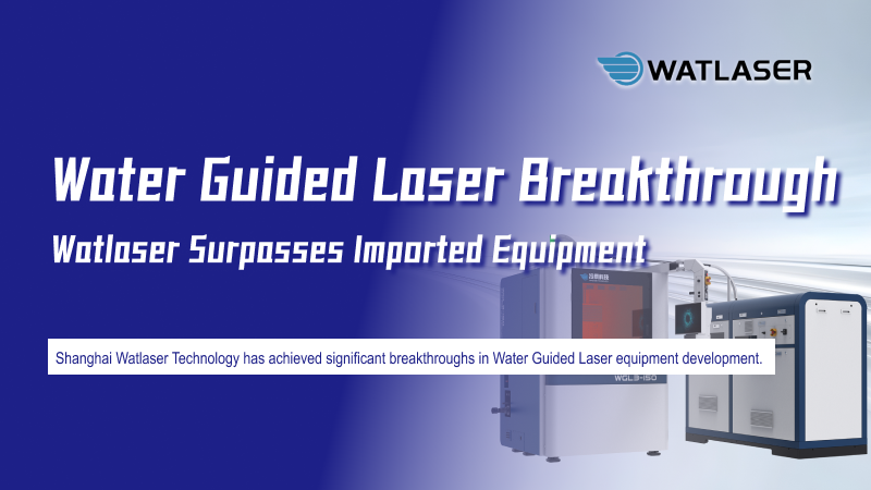
Water Guided Laser Technology Breakthrough: Watlaser Surpasses Imported Equipment
Water Guided Laser is emerging as a next-generation precision manufacturing technology for advanced materials and high-end industrial applications.
2025-09-28
-
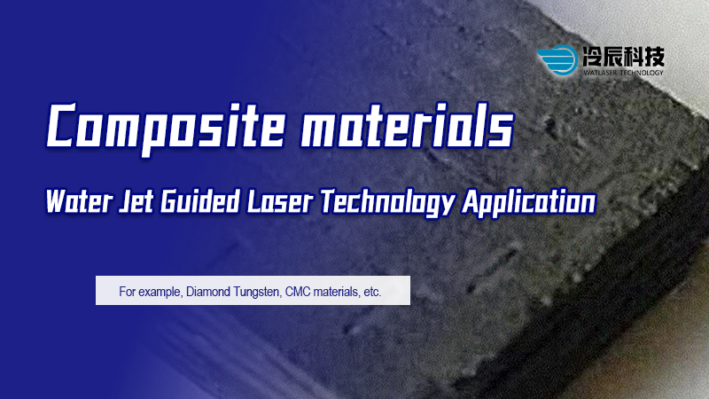
Composite Material
Such as doped diamond tungsten-based materials, CMC materials, etc.
2025-03-20
Precision Starts with Water Guided Laser
From CMC and CFRP composites to SiC ceramics and advanced aerospace materials, Watlaser provides Water Guided Laser solutions designed for high-precision, low-thermal-damage manufacturing. Explore Water Guided Laser Solutions for Aerospace Applications
Watlaser Technology develops and manufactures Water Guided Laser systems for precision machining of advanced materials. With in-house expertise in CNC systems, optical coupling, fluid control, and core hardware, Watlaser provides high-precision processing solutions for semiconductor, diamond, aerospace, medical, and industrial applications.

