

Water Guided Laser Processing for Microelectronics and Semiconductor Manufacturing
As manufacturing industries demand increasingly high-precision and high-efficiency processing technologies, Water Guided Laser (WGL) processing is attracting growing attention, particularly in microelectronics and semiconductor manufacturing.
These industries require extremely high levels of dimensional accuracy, surface quality, and material integrity. Conventional machining methods can struggle to meet these requirements, especially when processing hard and brittle semiconductor materials.
Water Guided Laser combines a laser beam with a high-speed water jet to create a unique precision processing method. The water jet guides the laser along the cutting path while simultaneously cooling the processing zone.
This approach can produce highly consistent, near-parallel kerfs while significantly reducing thermal effects during laser processing. As a result, it helps minimize thermal damage to sensitive components and improves overall processing quality, reliability, and performance.
Water Guided Laser technology has been explored internationally for precision drilling applications, particularly in demanding industrial sectors.
A representative application is the machining of film-cooling holes in turbine blades, where precision, hole quality, and process stability are critical.
Compared with conventional laser drilling, Water Guided Laser can produce holes with smoother edges and significantly less burr formation.
Conventional Laser Drilling
-
Rougher hole edges
-
Greater thermal effects
-
Potential recast and burr formation
-
Additional finishing may be required
Water Guided Laser Drilling
-
Smoother hole edges
-
Reduced thermal damage
-
Minimal burr formation
-
Improved overall hole quality
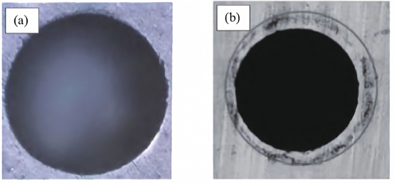
Figure 1. Comparison of (a) conventional laser drilling and (b) Water Guided Laser drilling.
The combination of laser precision and water cooling provides a significant advantage for applications requiring high-quality microholes and tight dimensional control.
When processing hard, brittle, or potentially hazardous semiconductor materials, manufacturers may face challenges such as workpiece movement, edge damage, debris generation, and airborne particulate contamination.
Water Guided Laser processing can help address these challenges while improving cutting quality and productivity.
One example is the precision cutting of gallium arsenide (GaAs) wafers.
Compared with conventional precision sawing, Water Guided Laser cutting can produce cleaner and more uniform kerfs with significantly less burrs and debris.
According to comparative research cited in the original article, Water Guided Laser cutting of GaAs wafers achieved cutting speeds approximately 7–10 times higher than precision sawing.
At the same time, the water jet helps capture and remove processing debris, reducing the risk of hazardous GaAs particles becoming airborne and contributing to a cleaner and safer manufacturing environment.
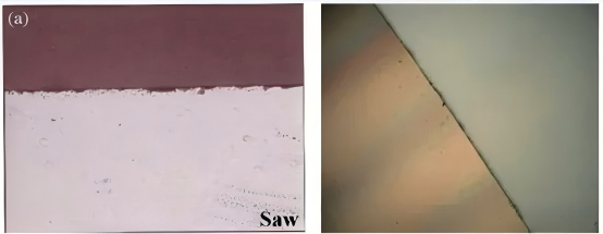
Figure 2. Comparison of front-surface quality between precision sawing and Water Guided Laser cutting of GaAs wafers.
Key Benefits for Semiconductor Cutting
-
High cutting efficiency
-
Clean and uniform kerfs
-
Reduced burrs and debris
-
Reduced thermal damage
-
Improved process cleanliness
-
Better suitability for hard and brittle semiconductor materials
Beyond cutting and drilling, Water Guided Laser technology can also be used to fabricate micro- and three-dimensional structures through precise control of the laser scanning path.
By controlling the cutting trajectory of the Water Guided Laser, periodic microstructures can be created directly on semiconductor materials.
For example, research has demonstrated the fabrication of periodic spiral grooves on silicon wafers using an inward-to-outward spiral scanning path.
The resulting grooves showed good overall processing quality with no significant molten material or recast inside the channels. The groove width was approximately 80 μm.
Water Guided Laser can also create three-dimensional microstructures by applying evenly spaced horizontal and vertical scanning paths.
Using this approach, pyramid-shaped structures with top dimensions as small as approximately 10 × 10 μm can be produced.
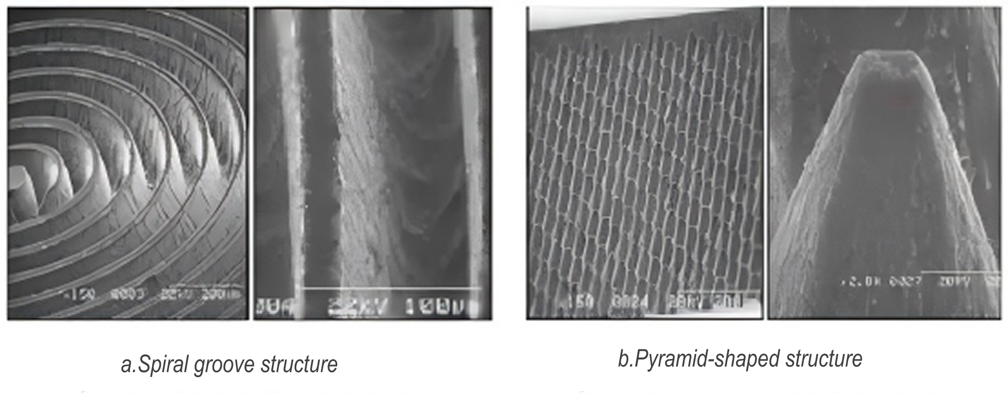
Figure 3. Microstructures fabricated using Water Guided Laser processing.
Microstructure Processing Capabilities
-
Precision micro-groove fabrication
-
Periodic surface structures
-
Three-dimensional microstructures
-
Fine feature processing
-
Reduced molten material and thermal damage
These capabilities make Water Guided Laser a promising technology for advanced semiconductor processing, microelectronics, MEMS-related manufacturing, and other precision microfabrication applications.
Compared with conventional laser processing, Water Guided Laser technology offers significant advantages in precision manufacturing, particularly for applications involving hard, brittle, and thermally sensitive materials.
Its combination of laser energy and water-jet cooling can provide:
-
High processing efficiency
-
High machining precision
-
Excellent surface quality
-
Reduced thermal damage
-
Clean and controlled processing
-
Improved suitability for hard and brittle materials
These advantages create new opportunities for the processing of advanced semiconductor materials such as silicon and silicon carbide (SiC), as well as other precision microelectronic components.
As semiconductor manufacturing continues to move toward smaller features, higher precision, and increasingly demanding material requirements, Water Guided Laser technology is expected to play an increasingly important role in high-precision cutting, drilling, and microstructure fabrication.


