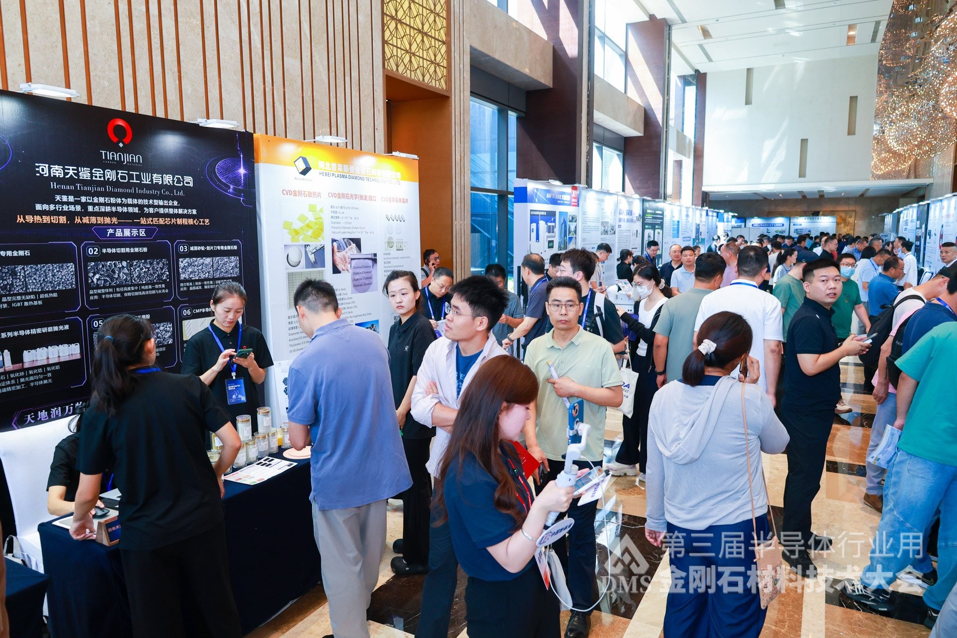

Exhibition Review | Watlaser participated in The 3rd Diamond Materials Technology for the Semiconductor Industry Conference
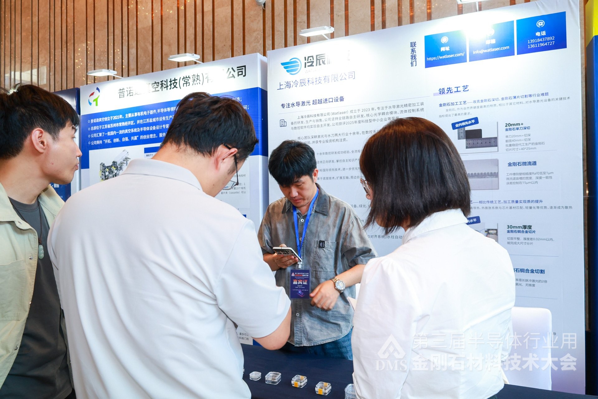
The 3rd Diamond Materials Technology Conference for the Semiconductor Industry & Power Semiconductor Technology Application and Equipment Seminar was successfully held in Zhengzhou, Henan, China, on September 3–4, 2026.
Watlaser participated in the event with its Water Guided Laser diamond processing solutions, engaging with industry experts and professionals to explore advances in diamond heat-spreader processing and the future of diamond materials in semiconductor applications.
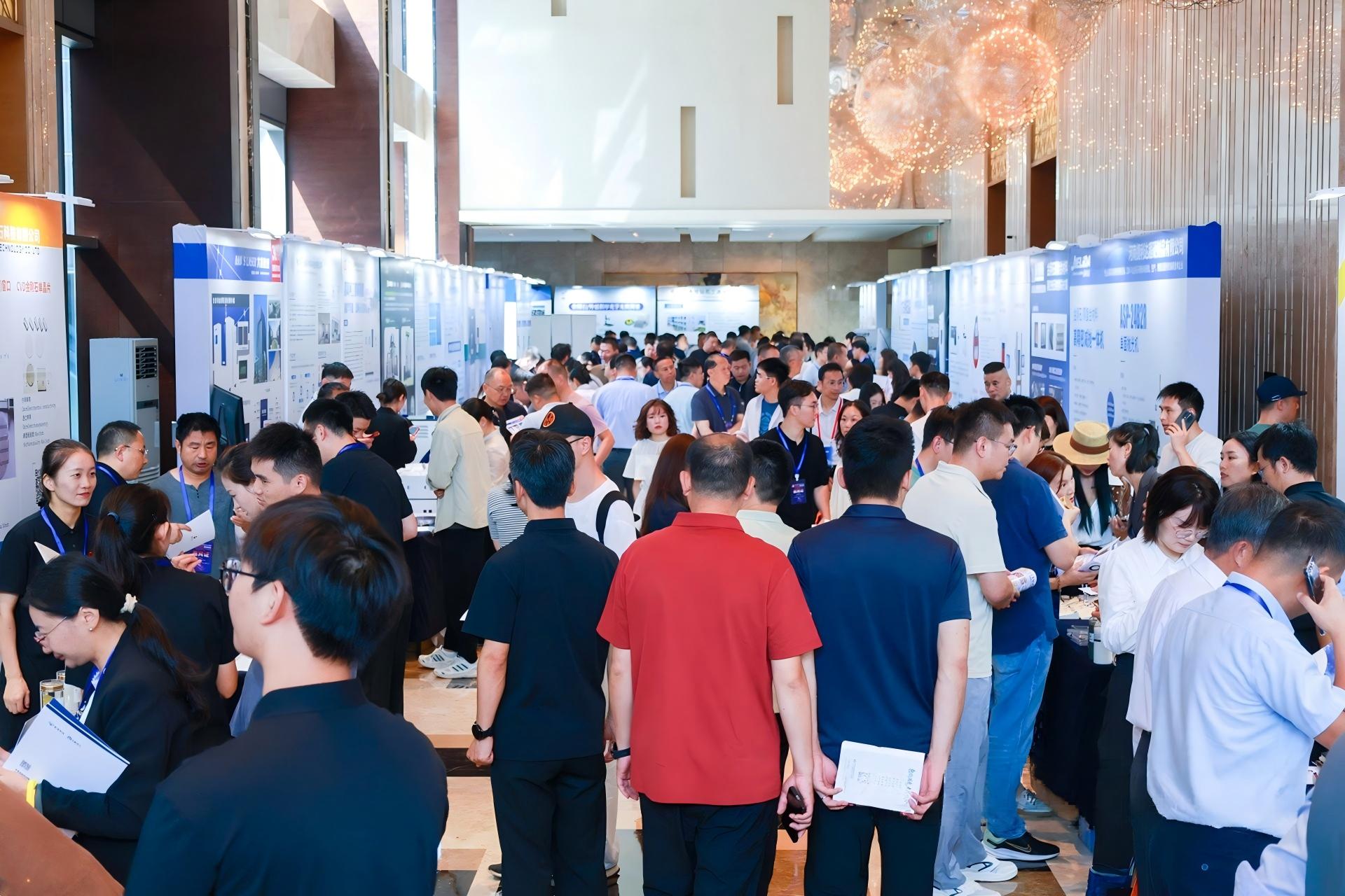
Diamond: A Key Material for Advanced Thermal Management
With the rapid development of power semiconductors and AI computing chips, diamond is emerging as a critical material for advanced thermal management thanks to its exceptionally high thermal conductivity.
Organized by Zhongfen Exhibition, the conference focused on the preparation, processing, and equipment technologies of diamond materials for semiconductor applications. It brought together companies, experts, and researchers from across the industry.
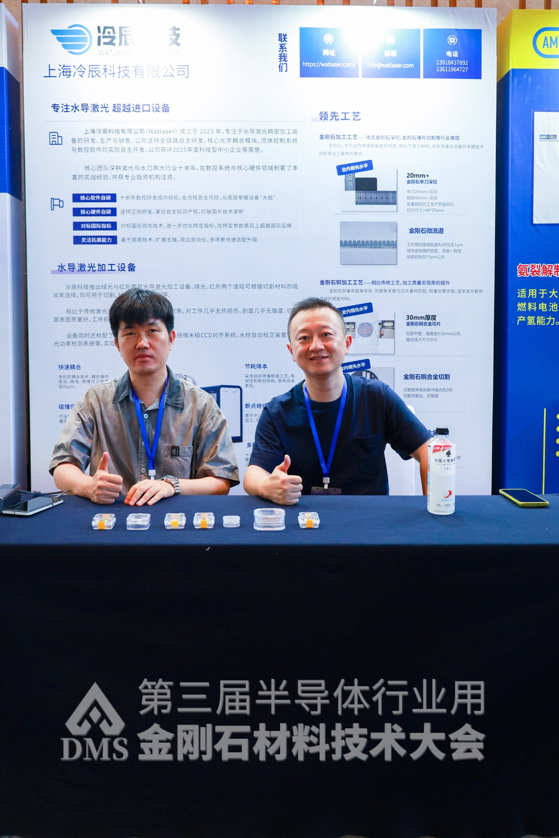
As a specialized company in Water Guided Laser precision processing, Watlaser presented its latest diamond processing technologies and solutions at the exhibition, attracting professionals from the semiconductor and thermal management industries.
Water Guided Laser for High-Precision Diamond Processing
Compared with conventional laser processing, Water Guided Laser technology guides high-energy laser light through a stable water jet, helping overcome common challenges in diamond processing, including:
-
Thermal damage
-
Excessive taper
-
Edge chipping
-
High material loss
This enables high-efficiency, low-loss and near-zero-taper precision processing for advanced diamond materials.
During the event, Watlaser’s technical team discussed three key processing technologies with visiting experts.
Diamond places extremely high demands on the core performance of Water Guided Laser processing equipment. Among these requirements, single-pass cutting depth is one of the key indicators of a system's diamond processing capability.
Watlaser’s proprietary Water Guided Laser technology has achieved:
20mm+ single-pass cutting depth
and
40mm+ cutting depth with double-sided processing.
This capability represents an advanced level of diamond deep-cutting technology in China.
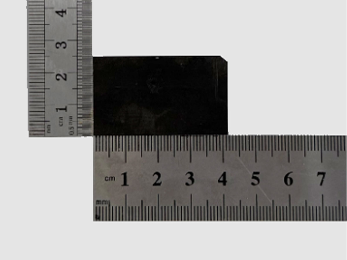
 Image Caption: Diamond wafers with dimensions greater than 40 × 25 mm produced through stable batch processing by Watlaser.
Watlaser’s Water Guided Laser technology enables precision machining of microchannels in diamond materials.
After processing:
-
No visible cracks
-
Surface roughness as low as Ra 1 μm
-
Width and depth consistency within 15 μm
This technology addresses key challenges in precision diamond microstructure processing, including material damage and excessive surface roughness.
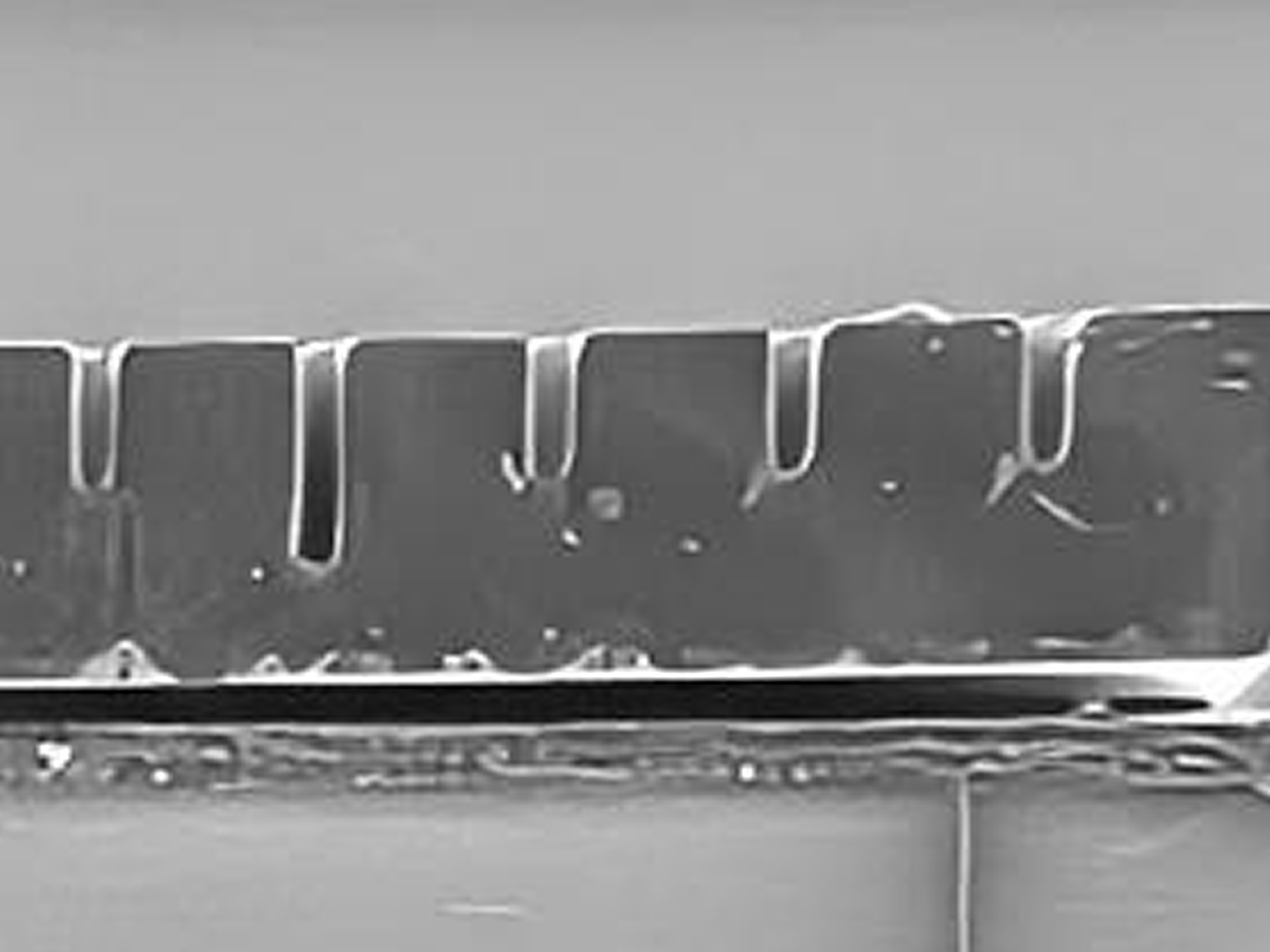
Image Caption: Diamond microchannel workpiece processed by Watlaser.
Watlaser has continuously optimized its diamond-copper processing technology through multiple generations of process development.
With its third-generation process, Watlaser can maintain a smooth cutting surface while achieving almost no diamond shedding.
The technology delivers:
20mm+ single-pass cutting depth
and effectively supports the processing requirements of various diamond-copper thermal management components.
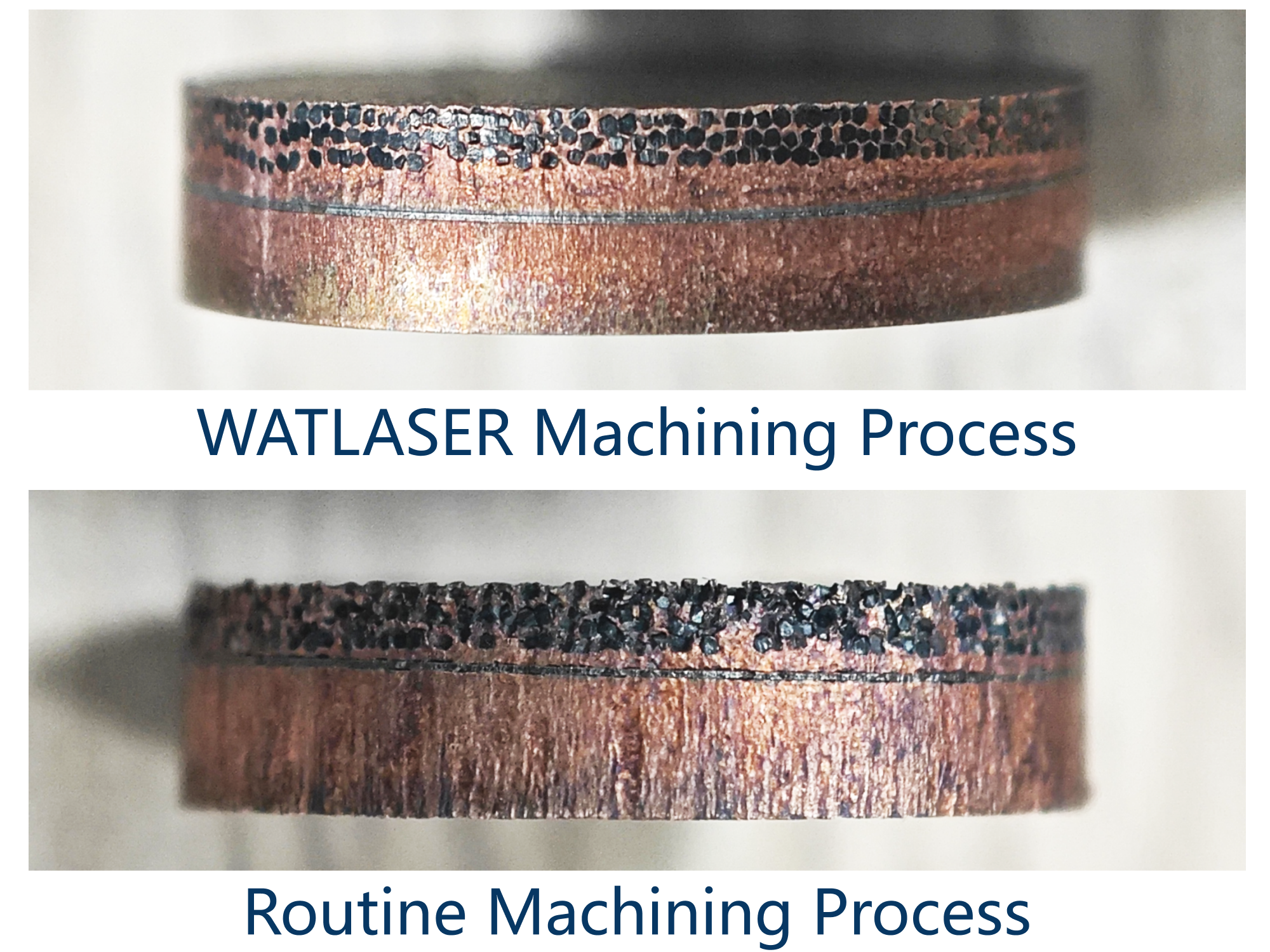
 Image Caption: Comparison of diamond-copper cutting surfaces processed using Watlaser technology and conventional processing methods.
Connecting Technology with Industry Applications
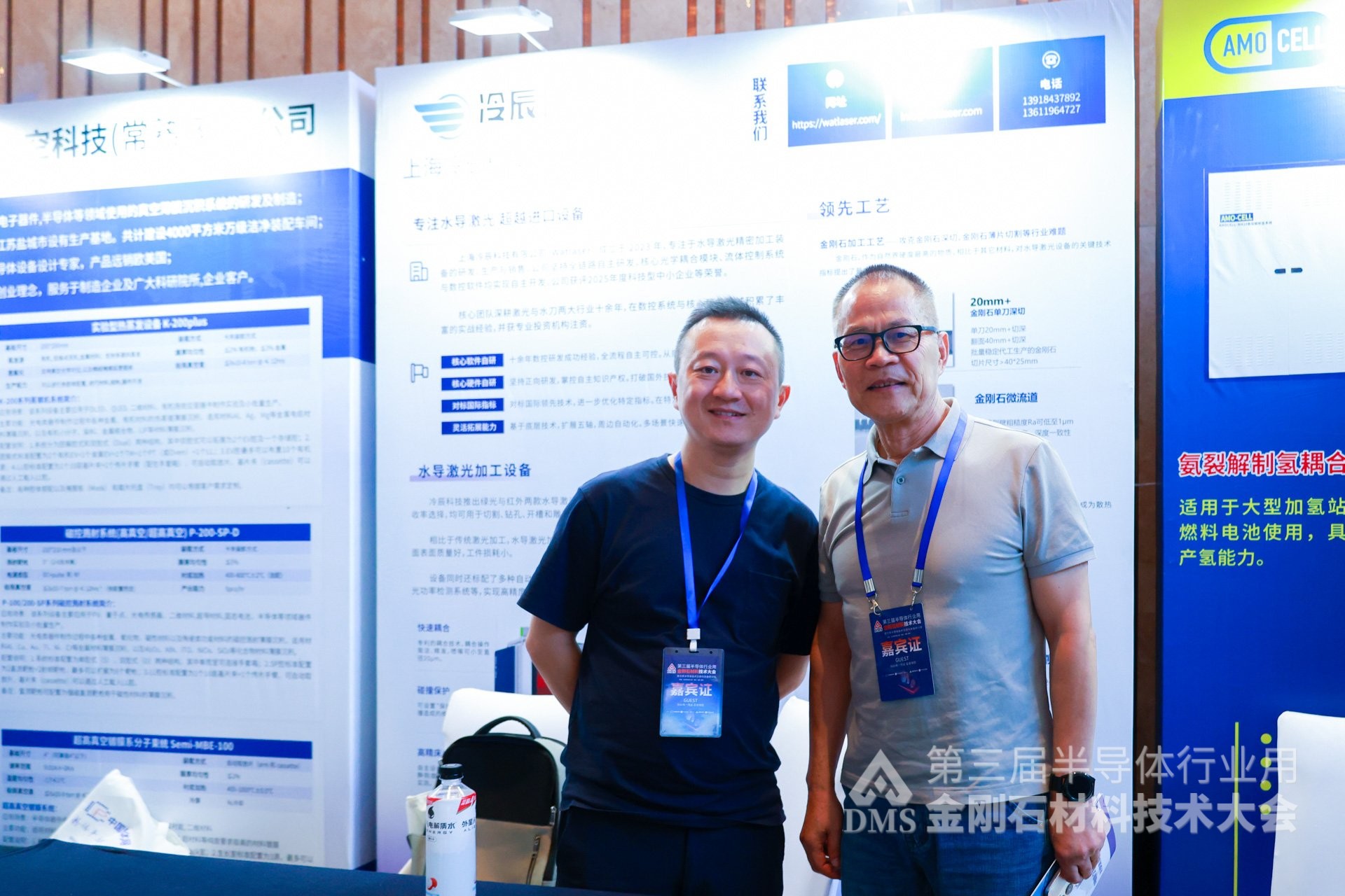
Throughout the conference, Watlaser’s booth attracted strong interest from professionals in semiconductor materials, power devices, thermal management, and research institutions.
Visitors engaged with the Watlaser team on topics including:
-
Processing efficiency
-
Cutting surface quality
-
Equipment stability
-
Diamond material processing
-
Diamond-copper thermal management components
Several industry experts recognized Watlaser’s advances in 20mm+ diamond deep cutting and diamond-copper processing, while expressing interest in further technical cooperation and sample trials.
Watlaser will continue to advance Water Guided Laser technology and provide high-precision processing solutions for diamond, diamond-copper composites, and other advanced materials used in semiconductor and thermal management applications.