

Exhibition Preview | Watlaser to Exhibit at the 3rd Diamond Materials Technology for the Semiconductor Industry Conference
From September 3 to 4, 2026, the 3rd Diamond Materials Technology for the Semiconductor Industry Conference & Power Semiconductor Technology Application and Equipment Seminar will be held in Zhengzhou, Henan, China.
Watlaser will participate in the event with its Water Guided Laser Diamond Processing Solutions, showcasing advanced technologies for high-efficiency and high-precision diamond machining.
We warmly welcome industry professionals to visit Booth A13 and explore the latest breakthroughs in diamond processing for semiconductor applications.
Diamond places extremely demanding requirements on Water Guided Laser processing capabilities.
Among these requirements, single-pass cutting depth is one of the key indicators of a system's ability to process thick diamond materials.
With its self-developed Water Guided Laser technology, Watlaser has achieved:
-
20mm+ single-pass cutting depth
-
40mm+ cutting depth with two-sided processing
-
Advanced processing capability for thick diamond materials
This technology represents a leading level of diamond processing capability in China.
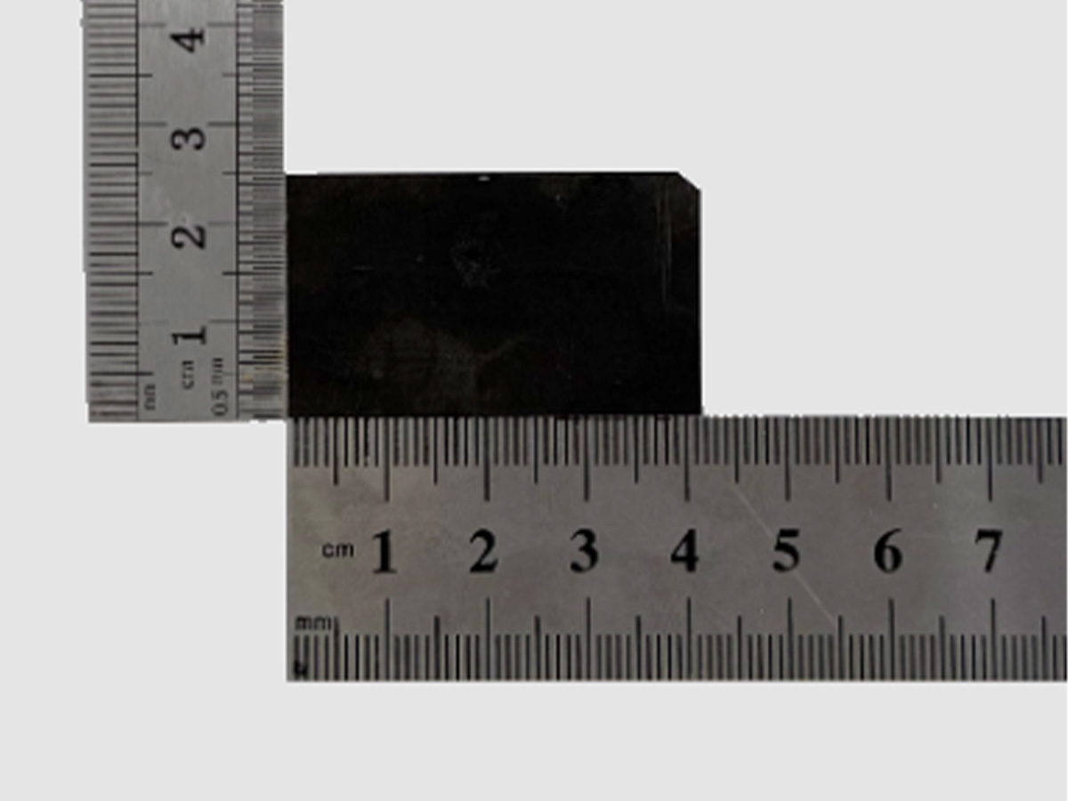
Image caption: Diamond cutting pieces with dimensions greater than 40 × 25 mm, stably produced in batch processing by Watlaser.
Watlaser's Water Guided Laser technology enables precision machining of microchannels in diamond materials.
After processing:
-
No visible cracks
-
Surface roughness of the channel can reach Ra ≤ 1 μm
-
Width and depth consistency error controlled within 15 μm
These capabilities address key challenges in diamond microstructure fabrication, including material damage, surface roughness, and dimensional inconsistency.
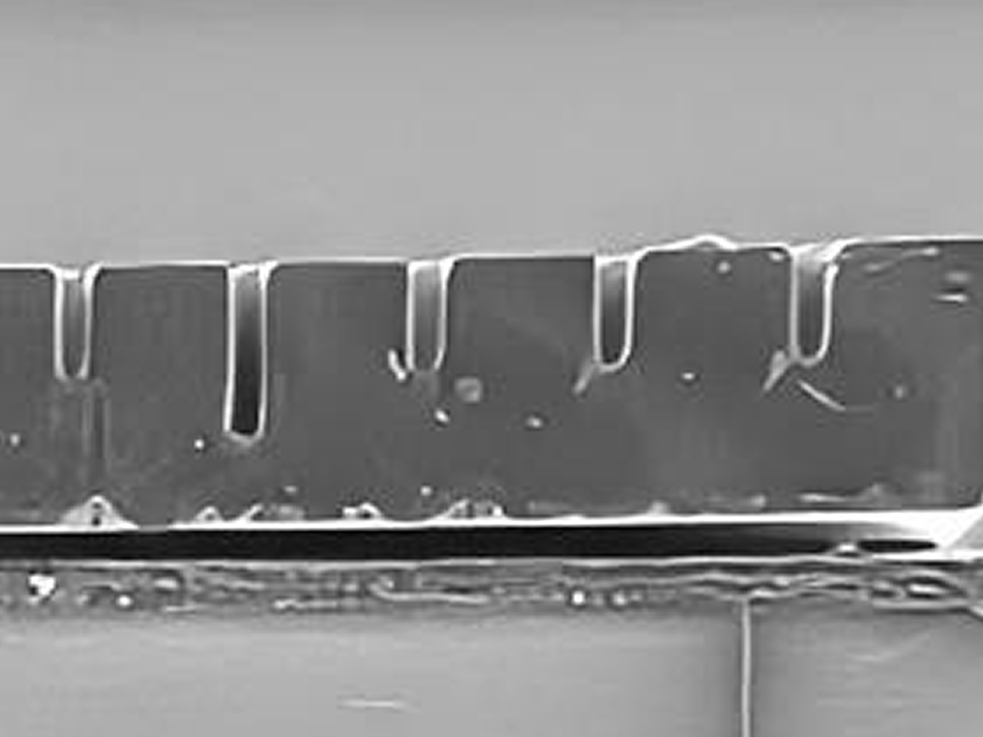
Image caption: Diamond microchannel workpiece processed by Watlaser.
Watlaser continues to optimize its diamond-copper cutting process through ongoing process development and technology iteration.
With the third-generation process, Watlaser can maintain a smooth cutting surface while achieving almost zero diamond shedding.
Key capability:
-
20mm+ single-pass cutting depth
-
Smooth cutting surfaces
-
Almost zero diamond shedding
-
Suitable for various advanced thermal management components
The process effectively addresses the demanding machining requirements of diamond-copper composite materials.

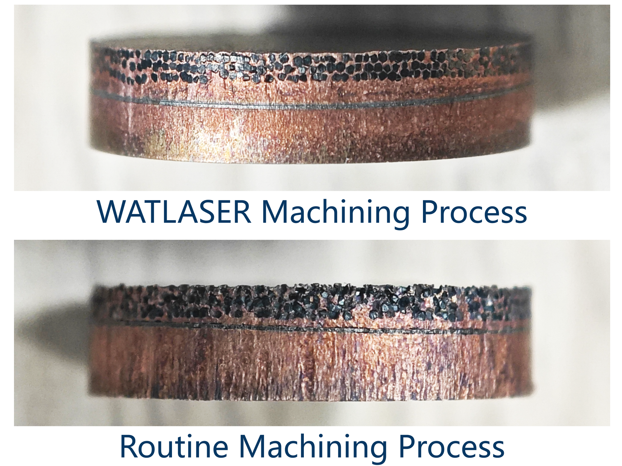 Image caption: Comparison of diamond-copper cutting surfaces processed using Watlaser's technology and a conventional process.
Enabling High-Efficiency, High-Precision Diamond Manufacturing
Backed by stable equipment performance, extensive process experience, and continuous technology development, Watlaser helps customers overcome critical diamond machining challenges.
Our Water Guided Laser solutions enable:
-
High Efficiency
Faster processing for demanding diamond applications. -
High Precision
Accurate machining with near-zero taper and controlled dimensional consistency. -
High Yield
Reduced material damage and improved processing quality for production applications.
Watlaser is committed to helping customers achieve efficient, high-precision and high-yield mass production of diamond materials, supporting the next generation of semiconductor and advanced thermal management technologies.
September 3–4, 2026 | Zhengzhou, Henan, China
Booth A13
We look forward to meeting you in Zhengzhou!


